
Full Wave Bridge Rectifier
1. Aim
To study the characteristics and performance of a Full Wave Bridge Rectifier, to analyze its input and output waveforms, and to determine its rectification efficiency and form factor.
2. Apparatus Used
- Step-down transformer (12V or 9V secondary)
- Four diodes (1N4007 or equivalent) for bridge configuration
- Load resistor (1kΩ, 2W)
- Breadboard/circuit board
- Connecting wires
- Cathode Ray Oscilloscope (CRO)
- AC voltmeter (0-15V range)
- DC voltmeter (0-15V range)
- AC ammeter or multimeter
- DC ammeter or multimeter
- Variac (optional, for variable input voltage)
3. Circuit Diagram
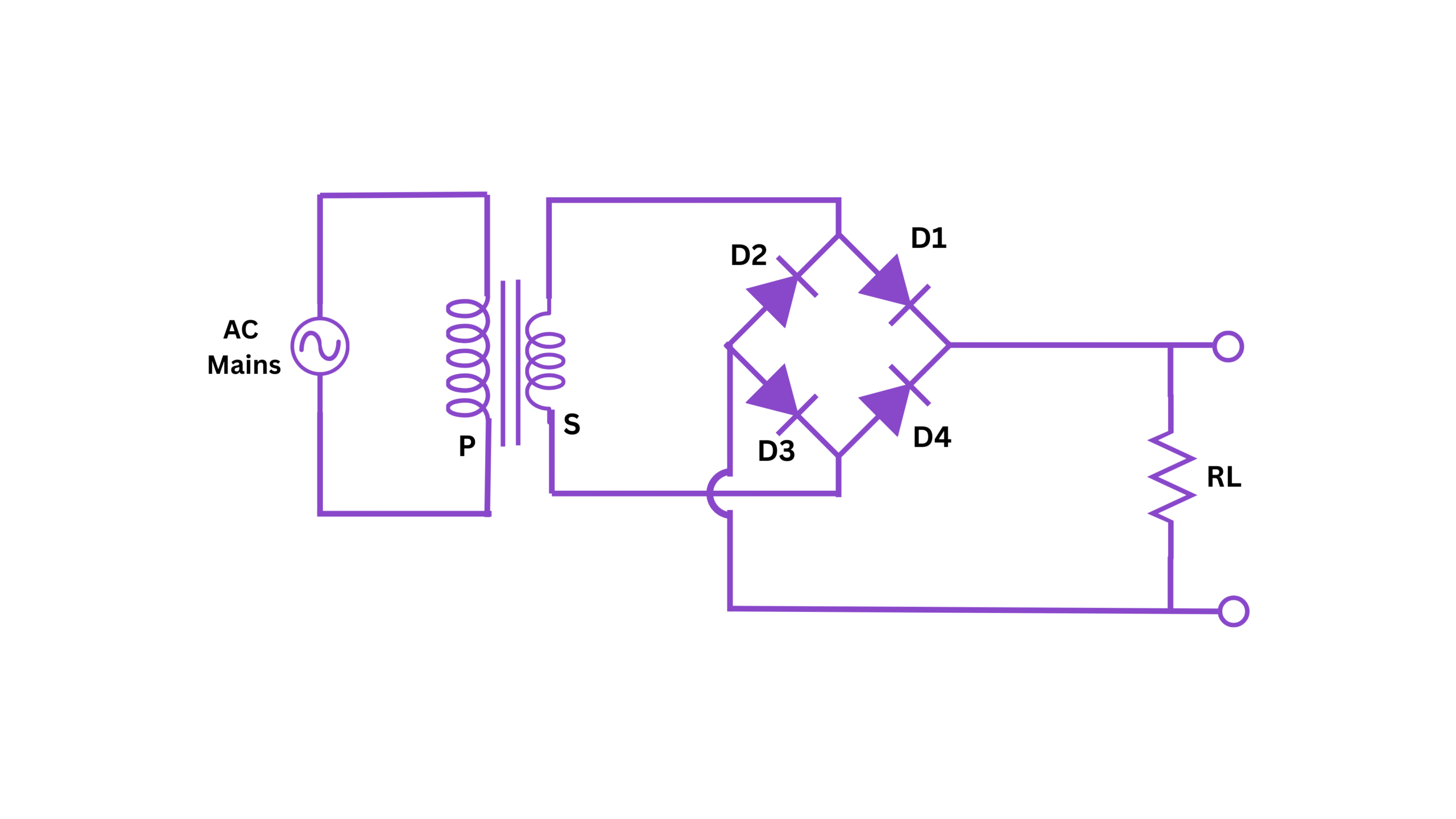
Fig 1: Full Wave Bridge Rectifier Circuit Diagram
4. Theory
A Full Wave Bridge Rectifier is an electronic circuit that converts alternating current (AC) to direct current (DC) by using the entire input waveform (both positive and negative half-cycles). It employs four diodes arranged in a bridge configuration to achieve full-wave rectification.
The bridge rectifier works on the principle of allowing current flow in only one direction through the load regardless of the polarity of the input AC voltage. During each half-cycle of the AC input, two diodes conduct while the other two are reverse-biased.
Operation during positive half-cycle:
When the input AC signal is in the positive half-cycle (top of transformer secondary is positive), diodes D1 and D3 are forward-biased and conduct current. Diodes D2 and D4 are reverse-biased and block current. The current path is: AC source → D1 → Load resistor → D3 → AC source.
Operation during negative half-cycle:
When the input AC signal is in the negative half-cycle (bottom of transformer secondary is positive), diodes D2 and D4 are forward-biased and conduct current. Diodes D1 and D3 are reverse-biased and block current. The current path is: AC source → D2 → Load resistor → D4 → AC source.
In both cases, the current flows through the load resistor in the same direction, producing a unidirectional (DC) voltage across it. This produces a full-wave rectified output which has the following characteristics:
- Frequency of output ripple is twice the input frequency
- No voltage output is lost (compared to center-tapped rectifier)
- Each diode conducts for 180° of the input cycle
- Two diode drops (2Vd) reduce the output voltage
Without a filter capacitor, the output waveform follows the absolute value of the sinusoidal input, producing a pulsating DC output that varies from zero to peak value.
5. Formulas
For a Full Wave Bridge Rectifier without filter:
RMS value of input voltage:
$V_{in(rms)} = \frac{V_{peak}}{\sqrt{2}}$
Average (DC) output voltage:
$V_{dc} = \frac{2V_m}{\pi} - 2V_d \approx 0.637V_m - 2V_d$
Where $V_m$ is the peak input voltage and $V_d$ is the diode forward voltage drop (typically 0.7V for silicon diodes)
RMS value of output voltage:
$V_{out(rms)} = \frac{V_m}{2}$
Ripple factor:
$r = \frac{\sqrt{V_{rms}^2 - V_{dc}^2}}{V_{dc}} = \sqrt{\frac{V_{rms}^2}{V_{dc}^2} - 1}$
For full wave rectifier, theoretical ripple factor = 0.482
Rectification efficiency:
$\eta = \frac{P_{dc}}{P_{ac}} \times 100\% = \frac{V_{dc}^2/R_L}{V_{rms}^2/R_L} \times 100\% = \frac{V_{dc}^2}{V_{rms}^2} \times 100\%$
Theoretical maximum efficiency for full wave rectifier = 81.2%
Form factor:
$\text{Form Factor} = \frac{V_{rms}}{V_{dc}}$
Ideal form factor for full wave rectifier = 1.11
Transformer Utilization Factor (TUF):
$\text{TUF} = \frac{P_{dc}}{P_{transformer}} = 0.812$
6. Procedure
- Connect the circuit as shown in the circuit diagram using four diodes in bridge configuration.
- Connect the step-down transformer's secondary to the AC input terminals of the bridge rectifier.
- Connect the load resistor (RL) across the DC output terminals of the bridge.
- Connect the AC voltmeter across the transformer secondary to measure input AC voltage.
- Connect the DC voltmeter across the load resistor to measure output DC voltage.
- Connect Channel 1 of the CRO to the transformer secondary (input) and Channel 2 to the load resistor (output).
- Turn on the power supply and adjust the input voltage (if using a variac) to the desired level (e.g., 12V AC).
- Observe and sketch the input and output waveforms displayed on the CRO.
- Measure the following parameters:
- Input AC voltage (RMS) using AC voltmeter
- Output DC voltage using DC voltmeter
- Input RMS current using AC ammeter
- Output DC current using DC ammeter
- Peak input voltage from CRO display
- Peak output voltage from CRO display
- Record all readings in the observation table.
- Repeat steps 7-10 for different values of input voltage (if required).
- Calculate the rectification efficiency, ripple factor, and form factor using the formulas provided.
- Compare the theoretical and experimental values of the calculated parameters.
- Turn off the power supply and disconnect the circuit.
7. Observation Table
| S.No. | Input AC | Output DC | ||||
|---|---|---|---|---|---|---|
| Voltage (Vin) (V) | Current (Iin) (mA) | Peak Voltage (Vm) (V) | Voltage (Vdc) (V) | Current (Idc) (mA) | Peak Voltage (Vp) (V) | |
| 1 | ||||||
| 2 | ||||||
| 3 | ||||||
| 4 | ||||||
| 5 | ||||||
| S.No. | RMS Output Voltage (Vrms) (V) |
Ripple Factor (r) |
Form Factor | Rectification Efficiency (η) (%) |
|---|---|---|---|---|
| 1 | ||||
| 2 | ||||
| 3 | ||||
| 4 | ||||
| 5 |
8. Calculations
For each set of observations, calculate the following parameters:
1. RMS Output Voltage:
Using the formula: $V_{out(rms)} = \frac{V_m}{2}$
Where $V_m$ is the peak input voltage.
2. Average DC Output Voltage (Theoretical):
Using the formula: $V_{dc} = \frac{2V_m}{\pi} - 2V_d \approx 0.637V_m - 2V_d$
Where $V_d$ is the diode forward voltage drop (typically 0.7V for silicon diodes).
3. Ripple Factor:
Using the formula: $r = \sqrt{\frac{V_{rms}^2}{V_{dc}^2} - 1}$
4. Form Factor:
Using the formula: $\text{Form Factor} = \frac{V_{rms}}{V_{dc}}$
5. Rectification Efficiency:
Using the formula: $\eta = \frac{V_{dc}^2}{V_{rms}^2} \times 100\%$
Sample Calculation: (To be filled with experiment data)
Let's say for observation 1:
- Input AC voltage (Vin) = ___ V
- Peak input voltage (Vm) = ___ V
- Output DC voltage (Vdc) = ___ V
Calculating RMS output voltage:
$V_{out(rms)} = \frac{V_m}{2} = \frac{\_\_\_}{2} = \_\_\_ \text{ V}$
Calculating ripple factor:
$r = \sqrt{\frac{V_{rms}^2}{V_{dc}^2} - 1} = \sqrt{\frac{(\_\_\_)^2}{(\_\_\_)^2} - 1} = \_\_\_$
Calculating form factor:
$\text{Form Factor} = \frac{V_{rms}}{V_{dc}} = \frac{\_\_\_}{\_\_\_} = \_\_\_$
Calculating rectification efficiency:
$\eta = \frac{V_{dc}^2}{V_{rms}^2} \times 100\% = \frac{(\_\_\_)^2}{(\_\_\_)^2} \times 100\% = \_\_\_\%$
9. Result
Based on the observations and calculations, the following results were obtained:
- The full wave bridge rectifier successfully converted AC input to pulsating DC output.
- Average DC output voltage (Vdc) = ___ V
- RMS output voltage (Vrms) = ___ V
- Ripple factor (r) = ___ (Theoretical value: 0.482)
- Form factor = ___ (Theoretical value: 1.11)
- Rectification efficiency (η) = ___% (Theoretical maximum: 81.2%)
The output waveform observed on the CRO shows full-wave rectification with frequency twice that of the input waveform. The bridge rectifier successfully rectifies both positive and negative half-cycles of the input AC signal.
The practical values obtained are [close to/differ from] the theoretical values due to [factors like diode voltage drops, resistive losses, or measurement errors].
10. Precautions
- Ensure all connections are tight and correctly made according to the circuit diagram.
- Verify the polarity of diodes before making connections.
- Use heat sinks with diodes if higher currents are involved.
- Do not exceed the voltage and current ratings of the diodes.
- Ensure that the load resistor has appropriate power rating.
- Turn off the power supply before making any changes to the circuit.
- Use appropriate range of measuring instruments to get accurate readings.
- Avoid loose connections as they may lead to errors in observations.
- Ensure proper grounding of the CRO to avoid electrical noise.
- Adjust the CRO settings properly to observe clear waveforms.
- Take multiple readings to ensure consistency and accuracy.
- Ensure that the transformer is properly rated for the experiment.
11. Viva Voice Questions
- What is the main advantage of a bridge rectifier over a center-tapped full wave rectifier?
A bridge rectifier does not require a center-tapped transformer and provides better transformer utilization. It also delivers a higher output voltage for the same input. - What is the PIV (Peak Inverse Voltage) rating of diodes in a bridge rectifier?
In a bridge rectifier, each diode must withstand a PIV equal to the peak value of the secondary voltage (Vm). - Why is the output frequency of a full wave rectifier twice the input frequency?
Because both positive and negative half-cycles of the input are converted to the same polarity at the output, resulting in two output pulses for each complete input cycle. - What is the difference between half-wave and full-wave rectification?
Half-wave rectification uses only one half (either positive or negative) of the input cycle, while full-wave rectification utilizes both halves, resulting in better efficiency and less ripple. - Why does the DC output voltage of a bridge rectifier have a lower value than the peak AC input voltage?
Due to two diode voltage drops (2Vd) in the current path and the fact that the average value of a sinusoidal waveform is less than its peak value. - What is ripple factor and why is it important?
Ripple factor is a measure of the AC component present in the rectified output. It's important because it indicates how effectively the rectifier converts AC to DC, with lower values indicating better performance. - How can the ripple in a rectifier output be reduced?
By adding filter circuits such as capacitor filters, inductor filters, or LC filters to smooth out the pulsating DC. - What would happen if one diode in the bridge rectifier fails (open circuit)?
The circuit would function as a half-wave rectifier, utilizing only one half-cycle of the input and reducing the output voltage and efficiency. - Why is the theoretical maximum efficiency of a full-wave bridge rectifier 81.2%?
This is due to the relationship between the RMS value and the average value of the rectified waveform, as well as power losses in the rectification process. - How does the form factor of a full wave rectified waveform compare to that of a pure sinusoidal wave?
The form factor of a full wave rectified waveform is 1.11, whereas for a pure sine wave it is 1.414.