
Transistor Characteristics in Common Emitter (CE) Configuration
Electronics Laboratory Experiment
1. Aim
To determine the input characteristics, output characteristics, and current gain characteristics of a Bipolar Junction Transistor (BJT) in Common Emitter (CE) configuration.
2. Apparatus Used
- Power supply (0-30V DC)
- Transistor (NPN/PNP) - BC107, 2N2222, or equivalent
- Ammeter (0-100mA DC)
- Microammeter (0-100μA DC)
- Voltmeter (0-20V DC) - 2 Nos.
- Rheostat (1kΩ, 2W) - 2 Nos.
- Connecting wires
- Breadboard
- Multi-turn potentiometers (10kΩ) - 2 Nos.
- Resistors: 1kΩ, 10kΩ
3. Circuit Diagram
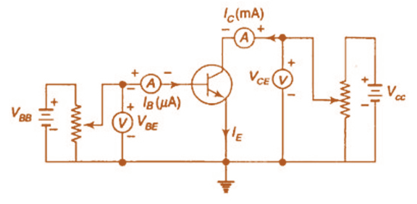
Figure 1: Circuit diagram of characteristics in Common Emitter (CE) Mode
4. Theory
A bipolar junction transistor (BJT) is a three-terminal semiconductor device consisting of two p-n junctions that can be used for amplification, switching, and signal generation. In the Common Emitter (CE) configuration, the emitter terminal is common to both input and output circuits.
The three terminals of a BJT are:
- Base (B): The thin, lightly doped center region
- Emitter (E): The heavily doped region that emits charge carriers
- Collector (C): The moderately doped region that collects charge carriers
BJTs come in two types: NPN and PNP, differing in their configuration of semiconductor materials. This experiment focuses on determining the characteristics of an NPN transistor in CE configuration.
Common Emitter Configuration:
In CE configuration, the emitter is common to both input and output circuits. The input signal is applied between base and emitter, and the output is taken across the collector and emitter. This configuration provides voltage, current, and power gain.
Transistor Characteristics in CE Mode:
- Input Characteristics: Graph of base current (IB) versus base-emitter voltage (VBE) at constant collector-emitter voltage (VCE).
- Output Characteristics: Graph of collector current (IC) versus collector-emitter voltage (VCE) at constant base current (IB).
- Current Transfer Characteristics: Graph of collector current (IC) versus base current (IB) at constant collector-emitter voltage (VCE).
Regions of Operation:
- Cutoff Region: Both junctions are reverse biased. Transistor acts as an open switch.
- Active Region: Base-emitter junction is forward biased, collector-base junction is reverse biased. Transistor operates as an amplifier.
- Saturation Region: Both junctions are forward biased. Transistor acts as a closed switch.
5. Formulas
Current Gain (β or hFE):
$ \beta = \frac{I_C}{I_B} $
Input Resistance (ri):
$ r_i = \frac{\Delta V_{BE}}{\Delta I_B} \text{ at constant } V_{CE} $
Output Resistance (ro):
$ r_o = \frac{\Delta V_{CE}}{\Delta I_C} \text{ at constant } I_B $
Transconductance (gm):
$ g_m = \frac{\Delta I_C}{\Delta V_{BE}} \text{ at constant } V_{CE} $
Transistor Power Dissipation:
$ P_D = V_{CE} \times I_C $
6. Procedure
A. Input Characteristics
- Connect the circuit as shown in the circuit diagram.
- Keep the collector-emitter voltage (VCE) constant (e.g., 5V) by adjusting rheostat RC.
- Vary the base-emitter voltage (VBE) from 0V to 0.8V in steps of 0.05V by adjusting rheostat RB.
- For each step, record the base current (IB) and base-emitter voltage (VBE).
- Repeat the procedure for different values of VCE (e.g., 10V, 15V).
B. Output Characteristics
- Keep the base current (IB) constant at a specific value (e.g., 10μA) by adjusting rheostat RB.
- Vary the collector-emitter voltage (VCE) from 0V to 10V in steps of 0.5V by adjusting rheostat RC.
- For each step, record the collector current (IC) and collector-emitter voltage (VCE).
- Repeat the procedure for different values of IB (e.g., 20μA, 30μA, 40μA, 50μA).
C. Current Transfer Characteristics
- Keep the collector-emitter voltage (VCE) constant (e.g., 5V) by adjusting rheostat RC.
- Vary the base current (IB) from 0μA to 100μA in steps of 10μA by adjusting rheostat RB.
- For each step, record the collector current (IC) and base current (IB).
- Repeat the procedure for different values of VCE (e.g., 10V).
7. Observation Tables
A. Input Characteristics
| Input Characteristics | ||||||
|---|---|---|---|---|---|---|
| Sl. No. | VCE = 5V | VCE = 10V | VCE = 15V | |||
| VBE (V) | IB (μA) | VBE (V) | IB (μA) | VBE (V) | IB (μA) | |
| 1 | ||||||
| 2 | ||||||
| 3 | ||||||
| 4 | ||||||
| 5 | ||||||
| 6 | ||||||
| 7 | ||||||
| 8 | ||||||
B. Output Characteristics
| Output Characteristics | |||||||||||
|---|---|---|---|---|---|---|---|---|---|---|---|
| Sl. No. | VCE (V) | IB = 10μA | IB = 20μA | IB = 30μA | IB = 40μA | IB = 50μA | |||||
| VCE (V) | IC (mA) | VCE (V) | IC (mA) | VCE (V) | IC (mA) | VCE (V) | IC (mA) | VCE (V) | IC (mA) | ||
| 1 | 0.0 | ||||||||||
| 2 | 0.5 | ||||||||||
| 3 | 1.0 | ||||||||||
| 4 | 1.5 | ||||||||||
| 5 | 2.0 | ||||||||||
| 6 | 2.5 | ||||||||||
| 7 | 3.0 | ||||||||||
| 8 | 3.5 | ||||||||||
| 9 | 4.0 | ||||||||||
| 10 | 4.5 | ||||||||||
| 11 | 5.0 | ||||||||||
C. Current Transfer Characteristics
| Current Transfer Characteristics | ||||
|---|---|---|---|---|
| Sl. No. | VCE = 5V | VCE = 10V | ||
| IB (μA) | IC (mA) | IB (μA) | IC (mA) | |
| 1 | 0 | 0 | ||
| 2 | 10 | 10 | ||
| 3 | 20 | 20 | ||
| 4 | 30 | 30 | ||
| 5 | 40 | 40 | ||
| 6 | 50 | 50 | ||
| 7 | 60 | 60 | ||
| 8 | 70 | 70 | ||
| 9 | 80 | 80 | ||
| 10 | 90 | 90 | ||
| 11 | 100 | 100 | ||
8. Calculations
A. Input Resistance (ri)
From the input characteristics curve, select two points (VBE1, IB1) and (VBE2, IB2) at a constant VCE, then calculate:
$ r_i = \frac{V_{BE2} - V_{BE1}}{I_{B2} - I_{B1}} $
Example: For VCE = 5V, if VBE1 = 0.65V, IB1 = 20μA and VBE2 = 0.7V, IB2 = 40μA
$ r_i = \frac{0.7 - 0.65}{40 \times 10^{-6} - 20 \times 10^{-6}} = \frac{0.05}{20 \times 10^{-6}} = 2.5 \text{ k}\Omega $
B. DC Current Gain (βDC)
From the current transfer characteristics, select a point (IB, IC) at a constant VCE, then calculate:
$ \beta_{DC} = \frac{I_C}{I_B} $
Example: For VCE = 5V, if IB = 30μA and IC = 3mA
$ \beta_{DC} = \frac{3 \times 10^{-3}}{30 \times 10^{-6}} = 100 $
C. Output Resistance (ro)
From the output characteristics curve, select two points (VCE1, IC1) and (VCE2, IC2) at a constant IB, then calculate:
$ r_o = \frac{V_{CE2} - V_{CE1}}{I_{C2} - I_{C1}} $
Example: For IB = 30μA, if VCE1 = 5V, IC1 = 3mA and VCE2 = 10V, IC2 = 3.1mA
$ r_o = \frac{10 - 5}{3.1 \times 10^{-3} - 3 \times 10^{-3}} = \frac{5}{0.1 \times 10^{-3}} = 50 \text{ k}\Omega $
D. Transconductance (gm)
Using the formula:
$ g_m = \frac{\beta}{r_i} $
Example: For β = 100 and ri = 2.5kΩ
$ g_m = \frac{100}{2.5 \times 10^3} = 40 \text{ mS} $
9. Result
From the experiment, the following parameters of the transistor in common emitter configuration have been determined:
- Input Resistance (ri) = _____ kΩ
- Output Resistance (ro) = _____ kΩ
- Current Gain (βDC) = _____
- Transconductance (gm) = _____ mS
The characteristics curves demonstrate the relationship between:
- Base current (IB) and base-emitter voltage (VBE) - Input Characteristics
- Collector current (IC) and collector-emitter voltage (VCE) - Output Characteristics
- Collector current (IC) and base current (IB) - Current Transfer Characteristics
The obtained characteristics curves confirm that the transistor operates in three distinct regions:
- Cut-off Region: Very low IC when IB is zero or very small
- Active Region: Linear relationship between IC and IB, with IC relatively insensitive to changes in VCE
- Saturation Region: IC no longer increases with IB, and is strongly dependent on VCE
10. Precautions
- Ensure all connections are correct before turning on the power supply.
- Start with minimum voltage and gradually increase to avoid damage to the transistor.
- Never exceed the maximum ratings of the transistor as specified in the datasheet.
- Ensure proper range selection in ammeters and voltmeters.
- Avoid short circuits, especially across the power supply.
- Handle the transistor carefully to avoid damage due to static electricity.
- Always connect the ammeter in series and voltmeter in parallel with the respective circuit elements.
- Turn off the power supply when making changes to the circuit.
- Keep the base current within safe limits to prevent excessive collector current.
- Allow sufficient time for readings to stabilize before recording them.
- Maintain the collector-emitter voltage within safe limits to prevent breakdown.
- Ensure proper heat dissipation for the transistor if operating at high power levels.
11. Viva Voice Questions
Q1: What is the common emitter configuration of a transistor?
Answer: In the common emitter configuration, the emitter terminal is common to both input and output circuits. The input signal is applied between the base and emitter, and the output is taken across the collector and emitter.
Q2: Why is common emitter configuration widely used in amplifier circuits?
Answer: Common emitter configuration is widely used because it provides voltage gain, current gain, and power gain simultaneously. It has moderate input impedance and output impedance, making it suitable for many applications.
Q3: What are the three regions of transistor operation in common emitter configuration?
Answer: The three regions are: Cutoff region (both junctions reverse biased), Active region (BE junction forward biased, BC junction reverse biased), and Saturation region (both junctions forward biased).
Q4: What is current amplification factor (β) and how is it calculated?
Answer: The current amplification factor (β) is the ratio of collector current to base current. It is calculated as β = IC/IB when the transistor is operating in the active region at a constant VCE.
Q5: Explain the early effect in transistors.
Answer: The Early effect is the variation in the effective width of the base due to variations in the applied collector-base voltage. This causes the collector current to increase slightly with increasing collector-emitter voltage, resulting in a finite slope of the output characteristics in the active region.
Q6: What causes saturation in a transistor?
Answer: Saturation occurs when both the base-emitter and base-collector junctions are forward biased. This happens when the base current is high enough that the collector current reaches its maximum value determined by the external circuit.
Q7: Why does the input characteristic curve of a transistor resemble a diode curve?
Answer: The input characteristic curve resembles a diode curve because the base-emitter junction is essentially a p-n junction diode. The current starts flowing significantly only after the base-emitter voltage exceeds the threshold voltage (typically 0.6-0.7V for silicon transistors).
Q8: How does the collector-emitter voltage affect the base current in a CE configuration?
Answer: In an ideal transistor, the collector-emitter voltage should not affect the base current. However, due to the Early effect, there is a slight increase in the base current with increasing VCE, which is visible in the input characteristics.
Q9: What is the significance of the knee voltage in output characteristics?
Answer: The knee voltage is the collector-emitter voltage at which the transistor transitions from the saturation region to the active region. Below the knee voltage, the transistor is in saturation, and above it, the transistor operates in the active region.
Q10: Compare the common emitter (CE) configuration with the common base (CB) and common collector (CC) configurations.
Answer:
common emitter (CE): Provides voltage gain, current gain, and power gain; 180° phase shift; moderate input and output impedances.
common base (CB): Provides voltage gain but current gain less than 1; no phase shift; low input impedance and high output impedance.
common collector (Emitter Follower): Provides current gain but voltage gain less than 1; no phase shift; high input impedance and low output impedance.