
Field Effect Transistor Characteristics
1. Aim
To study and determine the characteristics of a Field Effect Transistor by plotting:
- Drain characteristics (ID vs VDS for different values of VGS)
- Transfer characteristics (ID vs VGS at constant VDS)
2. Apparatus Used
| S.No. | Equipment/Component | Range/Specification | Quantity |
|---|---|---|---|
| 1 | N-channel JFET (e.g., 2N5457, BFW11) | TO-92 package | 1 |
| 2 | DC Power Supply | 0-30V, dual output | 1 |
| 3 | Digital Multimeter | Standard range | 2 |
| 4 | Resistors | 1kΩ, 100Ω | As required |
| 5 | Connecting wires | Standard | As required |
| 6 | Breadboard | Standard | 1 |
| 7 | Potentiometers | 10kΩ, 1kΩ | 2 |
3. Diagram
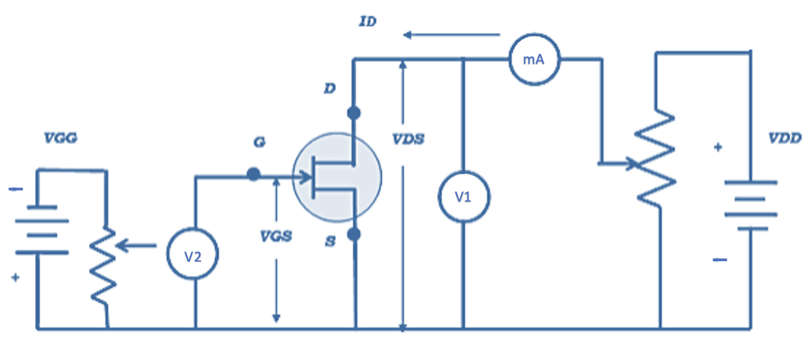
Fig 1: Circuit diagram for measuring FET characteristics
4. Theory
The Field Effect Transistor is a three-terminal semiconductor device that uses an electric field to control the flow of current. FETs are voltage-controlled devices, unlike BJTs which are current-controlled.
Types of FETs:
- Junction FET (JFET): Has a PN junction at the gate.
- Metal Oxide Semiconductor FET (MOSFET): Has an insulated gate structure.
Basic Structure and Working Principle:
A typical N-channel JFET consists of an N-type semiconductor channel with P-type regions (gates) on either side. The current flows from the drain to the source through this channel. The width of this channel, and thus the current flow, is controlled by the voltage applied to the gate terminal.
Key Characteristics:
1. Drain Characteristics: These show the relationship between drain current (ID) and drain-to-source voltage (VDS) for different values of gate-to-source voltage (VGS). The drain characteristics exhibit three distinct regions:
- Ohmic Region: At low VDS values, the FET behaves like a voltage-controlled resistor where ID increases linearly with VDS.
- Saturation Region: As VDS increases, the channel reaches a "pinch-off" point, and ID becomes nearly constant regardless of further increases in VDS.
- Breakdown Region: At very high VDS values, breakdown occurs and ID increases rapidly.
2. Transfer Characteristics: These show the relationship between drain current (ID) and gate-to-source voltage (VGS) at a constant drain-to-source voltage (VDS). For an N-channel JFET, ID decreases as VGS becomes more negative, eventually reaching a point called VGS(off) where the channel is completely pinched off and ID becomes zero.
3. Important Parameters:
- IDSS (Saturation Drain Current): The maximum drain current when VGS = 0 and VDS is in the saturation region.
- VGS(off) (Gate-Source Cutoff Voltage): The gate voltage at which the drain current effectively becomes zero.
- gm (Transconductance): A measure of the change in drain current with respect to a change in gate-source voltage, indicating the amplification capability.
- rd (Drain Resistance): The resistance of the channel in the saturation region.
5. Formula
The key formulas used in analyzing Field Effect Transistor characteristics are:
1. Shockley's Equation for JFETs in the saturation region:
$I_D = I_{DSS} \left(1 - \frac{V_{GS}}{V_{GS(off)}}\right)^2$
Where:
$I_D$ = Drain current
$I_{DSS}$ = Drain-source saturation current at $V_{GS} = 0$
$V_{GS}$ = Gate-source voltage
$V_{GS(off)}$ = Gate-source cutoff voltage
2. Transconductance ($g_m$):
$g_m = \frac{\partial I_D}{\partial V_{GS}} = \frac{-2 \times I_{DSS}}{V_{GS(off)}} \left(1 - \frac{V_{GS}}{V_{GS(off)}}\right)$
At $V_{GS} = 0$:
$g_{m0} = \frac{-2 \times I_{DSS}}{V_{GS(off)}}$
3. Drain Resistance ($r_d$):
$r_d = \frac{\partial V_{DS}}{\partial I_D}$
4. Amplification Factor ($\mu$):
$\mu = g_m \times r_d$
6. Procedure
A. Drain Characteristics (ID vs VDS for different VGS)
- Set up the circuit as shown in Fig. 1, ensuring all power supplies are initially set to zero.
- Connect the drain resistor RD (100Ω) in series with the drain terminal to protect the FET.
- Use a potentiometer to adjust VGS and another for VDS.
- Set VGS = 0V (connect gate directly to source).
- Vary VDS from 0V to 20V in steps of 1V and record the corresponding ID values.
- Set VGS = -0.5V and repeat step 5.
- Repeat the measurements for VGS = -1V, -1.5V, -2V, and -2.5V.
- For each set of readings, plot ID vs VDS to obtain the drain characteristics.
B. Transfer Characteristics (ID vs VGS at constant VDS)
- Using the same circuit setup, set VDS to a constant value in the saturation region (e.g., 15V).
- Vary VGS from 0V to -5V in steps of 0.25V (or until ID becomes effectively zero).
- Record the corresponding ID values for each VGS value.
- Plot ID vs VGS to obtain the transfer characteristics.
- From this graph, determine the value of VGS(off) where ID approaches zero.
- Calculate IDSS as the value of ID when VGS = 0V.
7. Observation Table
A. Drain Characteristics
| VDS (V) | Drain Current ID (mA) | ||||
|---|---|---|---|---|---|
| VGS = 0V | VGS = -0.5V | VGS = -1V | VGS = -1.5V | VGS = -2V | |
| 0 | |||||
| 1 | |||||
| 2 | |||||
| 3 | |||||
| 4 | |||||
| 5 | |||||
| 8 | |||||
| 10 | |||||
| 12 | |||||
| 15 | |||||
| 18 | |||||
| 20 | |||||
B. Transfer Characteristics (at constant VDS = 15V)
| VGS (V) | ID (mA) |
|---|---|
| 0 | |
| -0.25 | |
| -0.5 | |
| -0.75 | |
| -1.0 | |
| -1.25 | |
| -1.5 | |
| -1.75 | |
| -2.0 | |
| -2.5 | |
| -3.0 | |
| -3.5 | |
| -4.0 |
8. Calculations
From the observed data, perform the following calculations:
A. Calculate IDSS:
IDSS is the drain current when VGS = 0V and VDS is in saturation region (from drain characteristics plot).
IDSS = ID when VGS = 0V and VDS = 15V (or any value in saturation)
B. Determine VGS(off):
VGS(off) is the gate-source voltage at which the drain current becomes effectively zero (from transfer characteristics plot).
Find the x-intercept of the ID vs VGS curve
C. Calculate Transconductance (gm):
For any point on the transfer characteristic curve:
$g_m = \frac{\Delta I_D}{\Delta V_{GS}}$
For maximum transconductance (at VGS = 0V):
$g_{m0} = \frac{-2 \times I_{DSS}}{V_{GS(off)}}$
D. Calculate Drain Resistance (rd):
Select a point in the saturation region of drain characteristics:
$r_d = \frac{\Delta V_{DS}}{\Delta I_D}$ at constant VGS
E. Verify Shockley's Equation:
$I_D = I_{DSS} \left(1 - \frac{V_{GS}}{V_{GS(off)}}\right)^2$
Select a few points from transfer characteristics and compare the measured ID with the calculated ID using the equation.
Sample Calculation:
(Note: Fill this with actual sample calculation after obtaining experimental data)
9. Result
Based on the experiment, report the following:
- Successfully plotted the drain characteristics of the FET showing ID vs VDS for different values of VGS.
- Successfully plotted the transfer characteristics showing ID vs VGS at constant VDS.
- Determined the following parameters of the Field effect transistor:
| Parameter | Calculated Value | Datasheet Value (if available) |
|---|---|---|
| IDSS | ||
| VGS(off) | ||
| Maximum Transconductance (gm0) | ||
| Drain Resistance (rd) |
Conclusions about the behavior of the Field Effect Transistor based on observed characteristics:
- Observed the ohmic, saturation, and breakdown regions in the drain characteristics.
- Verified that the Field Effect Transistor behaves as a voltage-controlled current source in the saturation region.
- Validated the square-law relationship between ID and VGS as predicted by Shockley's equation.
10. Precautions
- Ensure proper identification of Field Effect Transistor terminals (Gate, Drain, Source) before making connections.
- Always use a protective resistor in series with the drain to limit current and prevent damage to the Field Effect Transistor.
- The gate of a JFET is essentially a reverse-biased PN junction. Never apply positive voltage to the gate of an N-channel JFET (or negative voltage to the gate of a P-channel JFET).
- Avoid exceeding the maximum ratings of the FET as specified in the datasheet.
- Make connections only when power supplies are off.
- Increase voltage gradually while taking readings to observe any anomalies in behavior.
- Field Effect Transistors are sensitive to static electricity. Handle them with care and use anti-static precautions if possible.
- Ensure accurate readings by allowing the circuit to stabilize before recording each measurement.
- Use calibrated instruments for accurate measurements.
- Double-check all connections before powering up the circuit.
11. Viva Voice Questions
Q1: What is the difference between a BJT and a FET?
Answer: BJT (Bipolar Junction Transistor) is a current-controlled device where the collector current is controlled by the base current. FET (Field Effect Transistor) is a voltage-controlled device where the drain current is controlled by the gate-source voltage. BJTs use both majority and minority carriers (bipolar) while FETs use only majority carriers (unipolar).
Q2: What are the advantages of FETs over BJTs?
Answer: FETs have higher input impedance (typically 10⁹ to 10¹⁵ ohms), lower noise, better thermal stability, greater ruggedness, no offset voltage at zero drain current, and they occupy less space in integrated circuits. They also exhibit no minority carrier storage effects, making them faster in switching applications.
Q3: Explain the meaning of the term "pinch-off" in a FET.
Answer: Pinch-off refers to the condition where the depletion regions from the gate junctions meet in the channel, causing the effective width of the channel to become extremely narrow. This occurs at a specific drain-source voltage (VP) for a given gate-source voltage. Beyond pinch-off, the drain current remains relatively constant despite increases in VDS, causing the FET to operate in the saturation region.
Q4: What is the significance of VGS(off) in a FET?
Answer: VGS(off), also known as the cutoff voltage, is the gate-source voltage at which the drain current becomes effectively zero. It represents the point at which the channel is completely pinched off due to the gate voltage alone, even with a positive VDS. This parameter is important in biasing FET circuits and determining the operating range.
Q5: What is transconductance in FETs and why is it important?
Answer: Transconductance (gm) is the ratio of a change in drain current to a change in gate-source voltage, with drain-source voltage held constant. It is measured in Siemens (S) or mho and indicates how effectively the gate voltage controls the drain current. Higher transconductance means better amplification capability, making it a crucial parameter for FET amplifier design.
Q6: Explain the different regions of operation in the drain characteristics of a FET.
Answer: The drain characteristics exhibit three main regions: (1) Ohmic region, where ID increases linearly with VDS; (2) Saturation region, where ID remains relatively constant despite increases in VDS; and (3) Breakdown region, where ID increases rapidly due to avalanche breakdown at high VDS values.
Q7: What is IDSS and how is it determined?
Answer: IDSS is the drain-to-source saturation current when VGS = 0 and VDS is in the saturation region. It represents the maximum drain current the FET can conduct with the gate shorted to the source. It is determined from the drain characteristics by measuring ID at VGS = 0 and at a VDS value in the saturation region.
Q8: Compare JFET and MOSFET.
Answer: JFETs have a PN junction at the gate while MOSFETs have an insulated gate with a metal oxide layer between the gate and channel. MOSFETs can operate in enhancement mode (normally OFF) or depletion mode (normally ON), while JFETs operate only in depletion mode. MOSFETs have even higher input impedance than JFETs, can be made smaller in ICs, and dominate modern digital electronics. JFETs are simpler in construction and generally more robust against static discharge.
Q9: What happens if the gate of an N-channel JFET is made positive with respect to the source?
Answer: If the gate of an N-channel JFET is made positive with respect to the source, the gate-channel PN junction becomes forward biased. This causes current to flow from gate to source, effectively destroying the isolation of the gate circuit. This condition should be avoided as it defeats the high input impedance advantage of the FET and may damage the device due to excessive gate current.
Q10: Explain the significance of Shockley's equation for FETs.
Answer: Shockley's equation ($I_D = I_{DSS} \left(1 - \frac{V_{GS}}{V_{GS(off)}}\right)^2$) describes the relationship between drain current and gate-source voltage in the saturation region. It shows that the drain current follows a square-law relationship with gate voltage. This equation is fundamental for analyzing and designing FET circuits, particularly biasing networks and amplifiers. It allows engineers to predict FET behavior based on datasheet parameters like IDSS and VGS(off).
Q11: Why does the drain current saturate in a FET after pinch-off?
Answer: After pinch-off, the channel near the drain end becomes extremely narrow. Any increase in VDS increases the electric field across this narrow region rather than widening the channel. Carriers injected from the source travel through the channel and get accelerated through this high-field region to the drain. Since the carrier injection rate from the source is controlled primarily by VGS (not VDS), the current remains relatively constant despite increases in VDS, leading to saturation.
Q12: How does temperature affect FET operation?
Answer: As temperature increases, the channel resistance increases due to decreased carrier mobility, leading to a reduction in IDSS. The VGS(off) also decreases slightly in magnitude. These effects cause a decrease in drain current at a given bias point. However, FETs have a negative temperature coefficient that helps prevent thermal runaway, making them more thermally stable than BJTs.