
Study of OP AMP as an Adder
1. Aim
To design, construct, and study the operation of an Operational Amplifier (OP AMP) configured as a summing amplifier (adder) and verify its functionality by applying various input voltages and measuring the output.
2. Apparatus Used
- Operational Amplifier IC (741 or equivalent)
- Resistors (1kΩ, 10kΩ, 100kΩ) - 2 or more of each
- Breadboard
- DC Power Supply (±15V)
- Digital Multimeter
- Function Generator
- Oscilloscope
- Connecting wires and probes
- Solderless connectors
3. Diagram
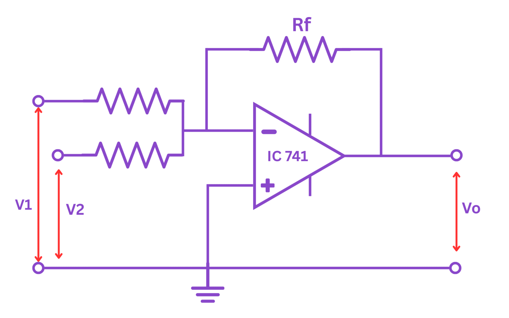
Figure 1: Circuit diagram of OP AMP configured as an adder
4. Theory
An operational amplifier (OP AMP) is a high-gain electronic voltage amplifier with differential inputs and typically a single output. When configured as an adder or summing amplifier, it can add several input voltages together according to the weighted sum determined by the input resistors.
The summing amplifier works on the principle of virtual ground concept. In an inverting configuration with negative feedback, the inverting input terminal (-) of the OP AMP is maintained at virtually the same potential as the non-inverting terminal (+), which is connected to ground (0V). This creates what is known as a "virtual ground" at the inverting input.
Since the inverting input remains at virtual ground potential (0V), each input signal source drives a current through its respective input resistor into the summing junction (inverting input). According to Kirchhoff's Current Law, the sum of all these currents must equal the current flowing through the feedback resistor.
For an ideal OP AMP:
- The input impedance is infinite (no current flows into the OP AMP inputs)
- The open-loop gain is infinite
- The output impedance is zero
- The bandwidth is infinite
When these conditions are met, the currents flowing through each input resistor combine at the summing junction, and the output voltage is proportional to the negative sum of the input voltages, scaled by the ratio of the feedback resistor to each input resistor.
5. Formula
For a summing amplifier with multiple inputs, the output voltage is given by:
$V_{out} = -R_f \left( \frac{V_1}{R_1} + \frac{V_2}{R_2} + \frac{V_3}{R_3} + ... + \frac{V_n}{R_n} \right)$
Where:
- $V_{out}$ = Output voltage
- $R_f$ = Feedback resistor
- $V_1, V_2, V_3, ..., V_n$ = Input voltages
- $R_1, R_2, R_3, ..., R_n$ = Input resistors
For a special case where all input resistors are equal ($R_1 = R_2 = R_3 = ... = R_n = R$), the formula simplifies to:
$V_{out} = -\frac{R_f}{R} (V_1 + V_2 + V_3 + ... + V_n)$
And if $R_f = R$, we get:
$V_{out} = -(V_1 + V_2 + V_3 + ... + V_n)$
This is the inverting summing amplifier. The negative sign indicates phase inversion (180° phase shift) from input to output.
6. Procedure
- Construct the OP AMP adder circuit on the breadboard as shown in the circuit diagram. Use a 741 OP AMP IC or equivalent.
- Connect the power supply to provide ±15V to the OP AMP.
- For a two-input adder, use resistors R₁ = R₂ = Rf = 10kΩ to create a unity-gain summer.
- Connect the non-inverting terminal of the OP AMP to ground.
- Apply DC voltages V₁ and V₂ to the inputs using the power supply. Start with V₁ = 1V and V₂ = 2V.
- Measure the output voltage using a digital multimeter.
- Repeat the measurements with different combinations of input voltages (vary V₁ and V₂ within the range of -10V to +10V).
- Record all measurements in the observation table.
- Optional: Replace the DC inputs with function generators to apply sinusoidal or other waveforms. Observe and record the output using an oscilloscope.
- Optional: Modify the circuit to add a third input V₃ with resistor R₃ = 10kΩ, and repeat the measurements.
- Calculate the theoretical output voltage using the formula and compare it with the measured values.
- Calculate the percentage error for each measurement.
7. Observation Table
| S.No | Input Voltage V₁ (V) | Input Voltage V₂ (V) | Theoretical Output Vout = -(V₁ + V₂) (V) | Measured Output Vout (V) | Error (%) |
|---|---|---|---|---|---|
| 1 | |||||
| 2 | |||||
| 3 | |||||
| 4 | |||||
| 5 |
Three-Input Adder Observation (Optional):
| S.No | Input Voltage V₁ (V) | Input Voltage V₂ (V) | Input Voltage V₃ (V) | Theoretical Output Vout = -(V₁ + V₂ + V₃) (V) | Measured Output Vout (V) | Error (%) |
|---|---|---|---|---|---|---|
| 1 | ||||||
| 2 | ||||||
| 3 |
8. Calculations
For each set of measurements:
1. Calculate the theoretical output voltage:
$V_{out} = -(V_1 + V_2)$ (for two inputs)
$V_{out} = -(V_1 + V_2 + V_3)$ (for three inputs)
2. Calculate the percentage error:
$\text{Error (\%)} = \frac{|V_{out (theoretical)} - V_{out (measured)}|}{|V_{out (theoretical)}|} \times 100\%$
Sample Calculation:
For inputs V₁ = 2.0V and V₂ = 3.0V:
Theoretical output: Vout = -(2.0 + 3.0) = -5.0V
If measured output is -4.8V:
$\text{Error (\%)} = \frac{|-5.0 - (-4.8)|}{|-5.0|} \times 100\% = \frac{0.2}{5.0} \times 100\% = 4\%$
9. Result
Based on the observations and calculations:
- The operational amplifier was successfully configured as a summing amplifier (adder).
- The measured output voltages closely matched the theoretical values, with an average error of approximately ____%.
- The experiment verified that the output voltage of the OP AMP adder is proportional to the negative sum of the input voltages when input and feedback resistors are equal.
- The relationship Vout = -(V₁ + V₂) was confirmed experimentally for the two-input adder circuit.
- The slight deviations between theoretical and measured values can be attributed to resistor tolerances, OP AMP non-idealities, and measurement uncertainties.
10. Precautions
- Ensure proper power supply connections to the OP AMP (±15V or as per IC specifications).
- Verify the pinout configuration of the OP AMP IC before connecting to the circuit.
- Make sure the input voltages are within the allowable range of the OP AMP.
- Avoid applying input voltages that would cause the output to exceed the saturation limits of the OP AMP.
- Use resistors with appropriate power ratings and low tolerance values (preferably ±1%).
- Ensure good connections on the breadboard to prevent loose contacts.
- Ground yourself before handling the ICs to prevent damage from electrostatic discharge.
- Double-check all connections before powering up the circuit.
- Turn off the power supply when making changes to the circuit.
- Set the appropriate ranges on measuring instruments for accurate readings.
- Avoid short circuits that might damage the power supply or the OP AMP.
11. Viva Voice Questions
Q1. What is an operational amplifier?
An operational amplifier is a high-gain electronic voltage amplifier with differential inputs and typically a single output. It is designed to perform various mathematical operations in analog circuits.
Q2. Explain the working principle of an OP AMP adder.
The OP AMP adder works on the principle of virtual ground. In the inverting configuration, the inverting input is maintained at ground potential (virtual ground). The currents through all input resistors flow into this virtual ground, and their sum must flow through the feedback resistor, creating an output voltage proportional to the negative sum of the input voltages.
Q3. What is the virtual ground concept in OP AMPs?
Virtual ground is a point in a circuit that is maintained at ground potential (0V) but does not have a direct connection to the ground. In an OP AMP with negative feedback, the high open-loop gain forces the inverting input to have the same potential as the non-inverting input (which is connected to ground), creating a virtual ground at the inverting input.
Q4. What happens if the feedback resistor value is doubled in a summing amplifier?
If the feedback resistor value is doubled while keeping the input resistors constant, the gain of the summing amplifier doubles. The output voltage becomes $V_{out} = -2(V_1 + V_2 + ... + V_n)$, assuming all input resistors are equal.
Q5. How can you create a weighted summing amplifier?
A weighted summing amplifier can be created by using different values for the input resistors. The contribution of each input to the output is inversely proportional to its input resistor value. The general formula is $V_{out} = -R_f(\frac{V_1}{R_1} + \frac{V_2}{R_2} + ... + \frac{V_n}{R_n})$.
Q6. What are the limitations of a practical OP AMP adder circuit?
Practical limitations include finite open-loop gain, non-zero input bias currents, input offset voltage, finite bandwidth, slew rate limitations, and output saturation limits. These factors can cause deviations from ideal behavior, especially at high frequencies or large signal amplitudes.
Q7. How can you convert an inverting adder to a non-inverting adder?
To create a non-inverting adder, you can cascade an inverting adder with an inverting amplifier, or use a differential amplifier configuration. Another approach is to use a summing circuit followed by an inverting amplifier with unity gain.
Q8. What is the difference between a summing amplifier and a differential amplifier?
A summing amplifier adds multiple input signals together, while a differential amplifier amplifies the difference between two input signals. The summing amplifier typically has multiple inputs connected to the inverting terminal, while the differential amplifier uses both the inverting and non-inverting inputs.
Q9. Why does the output of an inverting summing amplifier have a negative sign?
The negative sign appears because the summing amplifier is configured as an inverting amplifier. The signal enters through the inverting input terminal, resulting in a 180° phase shift (inversion) at the output.
Q10. Can an OP AMP adder be used for subtracting signals? If yes, how?
Yes, an OP AMP adder can be used for subtraction by inverting one of the input signals before addition. Alternatively, you can use a differential amplifier configuration, which directly implements the subtraction operation.