
To study the variation of voltage gain of a Common Emitter (CE) transistor amplifier with different load resistances and to analyze the relationship between gain and load resistance.
- NPN silicon transistor (BC107 or 2N2222)
- Resistors: 10kΩ, 1kΩ, 470Ω, and variable resistors (100kΩ, 10kΩ)
- Capacitors: 10μF, 100μF (electrolytic)
- DC power supply (0-15V)
- Function generator
- Dual trace oscilloscope
- Digital multimeter
- Breadboard and connecting wires
- Different load resistors (1kΩ, 2kΩ, 5kΩ, 10kΩ, 20kΩ)
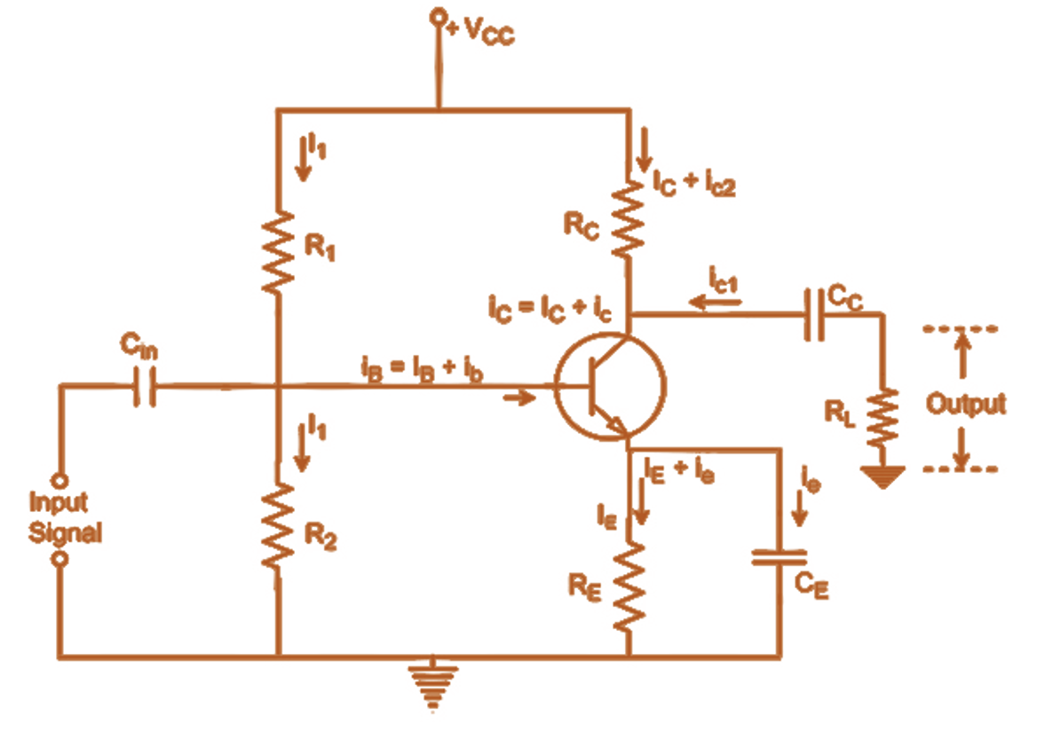
Fig. 1: Common Emitter Transistor Amplifier Circuit with Variable Load Resistance
A common emitter (CE) amplifier is a type of transistor amplifier configuration where the emitter of the transistor is common to both input and output circuits. The CE configuration is widely used because it provides good voltage, current, and power gain.
In this experiment, we focus on how the voltage gain of a CE amplifier varies with changes in the load resistance (RL). The voltage gain of a CE amplifier is defined as the ratio of the output voltage to the input voltage:
Av = Vout / Vin
The theoretical voltage gain of a CE amplifier depends on the transistor's transconductance (gm), the output resistance of the transistor (ro), and the load resistance (RL). For an AC signal, the voltage gain can be expressed as:
Av = -gm(RL || ro)
Where:
- gm is the transconductance of the transistor = IC/VT (VT ≈ 26mV at room temperature)
- ro is the output resistance of the transistor = VA/IC (VA is the Early voltage)
- RL is the load resistance
- (RL || ro) represents the parallel combination of RL and ro
For practical purposes, when RL is much smaller than ro, the gain becomes approximately:
Av ≈ -gmRL = -ICRL/VT
This shows that the voltage gain is directly proportional to the load resistance RL when other factors remain constant. As RL increases, the voltage gain increases linearly until RL becomes comparable to ro. At this point, the gain begins to saturate and approaches a maximum value of approximately -gmro.
The relationship between voltage gain and load resistance can be observed experimentally by varying RL and measuring the corresponding changes in voltage gain.
Voltage Gain (Av) = Vout / Vin
Theoretical Voltage Gain = -gm(RL || ro)
For small RL: Av ≈ -gmRL = -ICRL/VT
Where: VT ≈ 26mV at room temperature
Current Gain (β) = IC / IB
Transconductance (gm) = IC / VT
Parallel combination: RL || ro = (RL × ro) / (RL + ro)
- Set up the circuit as shown in the circuit diagram on the breadboard.
- Initially set the collector load resistance (RL) to 1kΩ.
- Apply a DC voltage of +10V to the collector through the collector resistor.
- Connect the function generator to the input of the amplifier circuit through the coupling capacitor C1.
- Set the function generator to produce a sinusoidal signal of frequency 1kHz with an amplitude of 20mV peak-to-peak.
- Connect channel 1 of the oscilloscope to the input (base) of the transistor and channel 2 to the output (collector).
- Measure and record the peak-to-peak voltage of both input (Vin) and output (Vout) signals.
- Calculate the voltage gain using the formula: Av = Vout / Vin
- Replace the load resistor with different values (2kΩ, 5kΩ, 10kΩ, 20kΩ) and repeat steps 7 and 8 for each value.
- Draw a graph of voltage gain (Av) versus load resistance (RL).
- Observe how the gain varies with the load resistance and verify the theoretical relationship.
| S.No. | Load Resistance RL (kΩ) | Input Voltage Vin (mVpp) | Output Voltage Vout (mVpp) | Voltage Gain Av = Vout/Vin |
|---|---|---|---|---|
| 1 | 1 | |||
| 2 | 2 | |||
| 3 | 5 | |||
| 4 | 10 | |||
| 5 | 20 |
For each load resistance value, calculate the voltage gain using the formula:
Av = Vout / Vin
For example, if with RL = 1kΩ:
Vin = 20mVpp and Vout = 240mVpp
Then, Av = 240mV/20mV = 12
To determine the relationship between gain and load resistance, plot a graph of Av versus RL. The graph should show an increasing trend initially, which may start to level off at higher load resistance values.
Additionally, we can calculate the theoretical voltage gain for each RL value using:
Av(theoretical) = -gm(RL || ro)
To calculate gm, measure the collector current IC:
gm = IC/VT = IC/26mV
Compare the experimental and theoretical values to analyze any discrepancies.
- The variation of voltage gain (Av) with load resistance (RL) was studied experimentally.
- It was observed that the voltage gain increases with increasing load resistance initially, following approximately a linear relationship.
- At higher load resistance values, the rate of increase in gain diminishes, showing a tendency to saturate.
- The experimental results [were/were not] in close agreement with the theoretical predictions, with a deviation of approximately [x]%.
- The maximum voltage gain achieved was [value] at a load resistance of [value] kΩ.
Note: Complete this section after performing the experiment with actual measured values.
- Ensure proper biasing of the transistor to avoid distortion of the output signal.
- Maintain the input signal amplitude small enough to prevent the amplifier from entering saturation or cutoff regions.
- Use coupling capacitors of appropriate values to ensure proper signal transfer at the frequency of operation.
- Ensure all connections are secure and correct before powering on the circuit.
- Avoid touching the circuit components when the power is on to prevent electric shock and circuit disturbance.
- Check the polarity of electrolytic capacitors and ensure they are connected correctly.
- Use the oscilloscope probes with proper ground connections to avoid measurement errors.
- Ensure the transistor does not overheat during the experiment by limiting the collector current.
- Verify the functionality of all components before assembling the circuit.
- Keep the input frequency within the bandwidth of the amplifier for accurate measurements.