
To Study Gain-Frequency Response of CE Transistor Amplifier
1. Aim
To design and set up a Common Emitter Transistor amplifier circuit and study its gain-frequency response characteristics.
2. Apparatus Used
- Transistor (2N2222 or BC547)
- Resistors (RC, RE, R1, R2)
- Capacitors (Cin, Cout, CE)
- Function Generator
- CRO (Cathode Ray Oscilloscope)
- DC Regulated Power Supply
- Connecting Wires
- Breadboard
- Digital Multimeter
3. Circuit Diagram
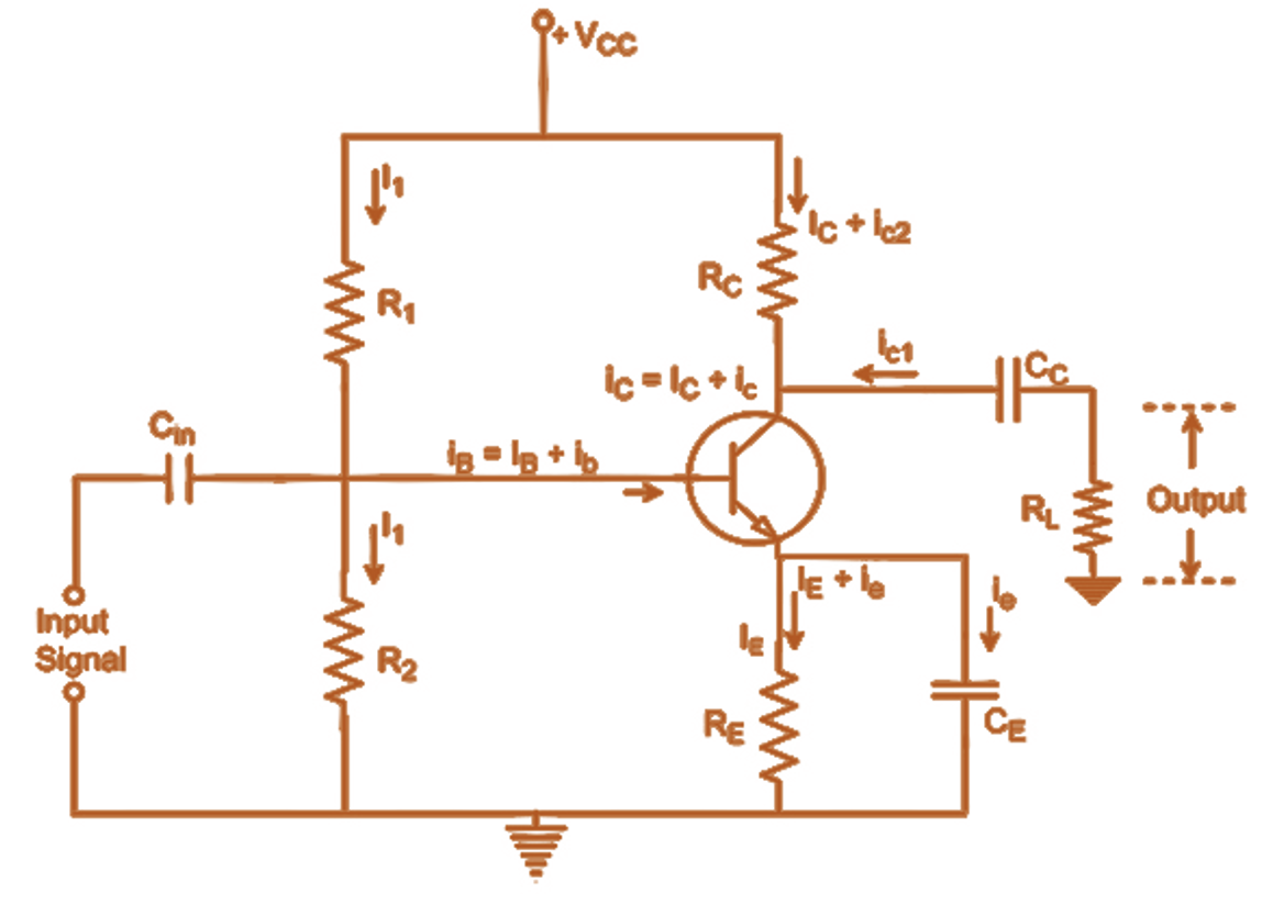
Fig 1: Common Emitter Transistor Amplifier Circuit
4. Theory
The Common Emitter amplifier is one of the most commonly used transistor amplifier configurations. In this configuration, the emitter terminal is common to both input and output circuits. The input signal is applied between the base and emitter, and the output is taken from the collector and emitter.
Key characteristics of a Common Emitter amplifier include:
- Voltage Gain: It provides high voltage gain.
- Current Gain: It provides moderate to high current gain.
- Power Gain: It provides high power gain.
- Input/Output Phase: There is a 180° phase shift between input and output signals.
The gain-frequency response of an amplifier shows how the amplifier's gain varies with frequency. There are three main regions in the frequency response:
- Low-frequency region: The gain drops at low frequencies due to the coupling and bypass capacitors.
- Mid-frequency region: This is the flat band region where the gain remains relatively constant. This is the desired operating region for the amplifier.
- High-frequency region: The gain drops at high frequencies due to internal transistor capacitances and stray capacitances.
The bandwidth of the amplifier is defined as the range of frequencies over which the voltage gain does not fall below 70.7% (or -3dB) of the maximum gain.
The coupling capacitors (Cin and Cout) are used to block DC while allowing AC signals to pass. The emitter bypass capacitor (CE) is used to bypass the AC signal around the emitter resistor, which increases the gain of the amplifier.
5. Formulas
Voltage Gain (Av):
$$A_v = \frac{V_{out}}{V_{in}} = \frac{R_C}{r_e + R_E}$$
where \(r_e\) is the AC emitter resistance given by:
$$r_e = \frac{25 mV}{I_E}$$
Lower Cutoff Frequency (fL):
Determined by coupling capacitors and bypass capacitor:
$$f_L = \frac{1}{2\pi RC}$$
where R and C represent the effective resistance and capacitance at low frequencies.
Upper Cutoff Frequency (fH):
Determined by internal transistor capacitances:
$$f_H = \frac{1}{2\pi R_C C_{eq}}$$
where \(C_{eq}\) is the equivalent capacitance at high frequencies.
Bandwidth (BW):
$$BW = f_H - f_L$$
Gain in Decibels (dB):
$$A_v (dB) = 20 \log_{10} |A_v|$$
6. Procedure
- Connect the circuit of Common Emitter Amplifier as shown in the circuit diagram.
- Set the DC power supply to provide VCC = 10V.
- Before connecting the input signal, verify the DC operating point of the transistor:
- Measure VBE (should be approximately 0.7V for silicon transistors)
- Measure VCE (should be approximately 40-60% of VCC)
- Measure IC by measuring voltage across RC and using Ohm's law
- Connect the function generator to provide a sinusoidal input signal of small amplitude (about 100mV peak-to-peak) to avoid clipping.
- Set the function generator to a frequency in the mid-band range (typically 1kHz).
- Observe the input and output waveforms on the CRO and note that they are 180° out of phase.
- Measure the input voltage (Vin) and output voltage (Vout) using the CRO.
- Calculate the voltage gain at this frequency using the formula Av = Vout/Vin.
- Maintaining the input signal amplitude constant, vary the frequency from 10Hz to 1MHz (or as per available equipment range) and record the output voltage for each frequency.
- Record all observations in the observation table.
- Plot a graph of voltage gain (in dB) versus frequency (logarithmic scale).
- From the graph, determine the lower cutoff frequency (fL), upper cutoff frequency (fH), and bandwidth (BW).
7. Observation Table
| S.No. | Frequency (Hz) | Input Voltage Vin (mV) | Output Voltage Vout (mV) | Voltage Gain Av = Vout/Vin | Gain in dB = 20 log10|Av| |
|---|---|---|---|---|---|
| 1 | 10 | ||||
| 2 | 20 | ||||
| 3 | 50 | ||||
| 4 | 100 | ||||
| 5 | 200 | ||||
| 6 | 500 | ||||
| 7 | 1k | ||||
| 8 | 2k | ||||
| 9 | 5k | ||||
| 10 | 10k | ||||
| 11 | 20k | ||||
| 12 | 50k | ||||
| 13 | 100k | ||||
| 14 | 200k | ||||
| 15 | 500k | ||||
| 16 | 1M |
8. Calculations
From the observation table and gain-frequency plot:
1. Determining the Mid-band Gain:
Find the maximum gain from the table. This is the mid-band gain.
Mid-band Gain (Av max) = ________ (linear)
Mid-band Gain in dB = 20 log10|Av max| = ________ dB
2. Determining Cutoff Frequencies:
Lower cutoff frequency (fL): Frequency at which gain drops to 0.707 times the mid-band gain.
Upper cutoff frequency (fH): Frequency at which gain drops to 0.707 times the mid-band gain.
In dB terms, cutoff frequencies occur where the gain drops by 3dB from the mid-band gain.
Lower cutoff frequency (fL) = ________ Hz
Upper cutoff frequency (fH) = ________ Hz
3. Calculating Bandwidth:
Bandwidth (BW) = fH - fL = ________ Hz
9. Result
Based on the experiment and calculations, the following results have been obtained:
- The maximum voltage gain (mid-band gain) of the Common Emitter amplifier is ________ (linear) or ________ dB.
- The lower cutoff frequency (fL) is ________ Hz.
- The upper cutoff frequency (fH) is ________ Hz.
- The bandwidth (BW) of the Common Emitter amplifier is ________ Hz.
- The gain-frequency response of the Common Emitter amplifier demonstrates the expected characteristics with gain decreasing at both low and high frequencies.
- The phase shift between input and output signals is observed to be 180°, which confirms the phase-inverting nature of the Common Emitter amplifier.
10. Precautions
- Ensure all connections are tight and correct before turning on the power supply.
- Use the correct polarity for the transistor and electrolytic capacitors.
- Keep the input signal amplitude small to avoid clipping of the output signal.
- Verify the DC operating point of the transistor before applying the input signal.
- Ensure the transistor does not overheat during the experiment.
- Avoid touching the circuit while it is powered on.
- Use proper grounding for all equipment to avoid measurement errors.
- Ensure the function generator and CRO are properly calibrated.
- Keep the input frequency constant while measuring the output voltage.
- Turn off the power supply before making any changes to the circuit.
11. Viva Voice Questions
Q1: What is the difference between CE, CB, and CC configurations of a transistor amplifier?
Answer: The main differences are:
- CE (Common Emitter): Emitter is common to both input and output circuits. It provides high voltage gain, high current gain, high power gain, and has a 180° phase shift.
- CB (Common Base): Base is common to both input and output circuits. It provides high voltage gain, less than unity current gain, moderate power gain, and no phase shift.
- CC (Common Collector): Collector is common to both input and output circuits. It provides unity (or slightly less) voltage gain, high current gain, moderate power gain, and no phase shift. It is also known as an emitter follower.
Q2: Why does the gain of a Common Emitter Amplifier decrease at low frequencies?
Answer: At low frequencies, the reactance of coupling capacitors (Cin and Cout) and bypass capacitor (CE) increases. This leads to signal attenuation across these capacitors, resulting in reduced gain. The coupling capacitors block some of the input signal, and the emitter bypass capacitor becomes less effective at bypassing the AC signal around the emitter resistor.
Q3: Why does the gain decrease at high frequencies?
Answer: At high frequencies, the internal transistor capacitances (junction capacitances like Cbe, Cbc, and Cce) and stray capacitances in the circuit become significant. These capacitances provide low-impedance paths for the signal, causing signal bypassing and reducing the gain. Additionally, the transistor's gain-bandwidth product and the Miller effect contribute to the high-frequency roll-off.
Q4: What is the role of the emitter bypass capacitor (CE) in a Common Emitter amplifier?
Answer: The emitter bypass capacitor (CE) is connected in parallel with the emitter resistor (RE). It bypasses the AC signal around RE, preventing AC degeneration. This significantly increases the voltage gain of the amplifier. However, RE still provides DC stabilization of the operating point, helping to stabilize the circuit against temperature changes and transistor parameter variations.
Q5: What is the significance of -3dB points in the frequency response of an amplifier?
Answer: The -3dB points are frequencies at which the power gain of the amplifier falls to half (50%) of its maximum value, which corresponds to a voltage gain reduction to 70.7% of the maximum. These points define the bandwidth of the amplifier. The range between the lower -3dB frequency (fL) and the upper -3dB frequency (fH) is considered the effective operational range of the amplifier.
Q6: What is the Miller effect and how does it affect the high-frequency response of a Common Emitter amplifier?
Answer: The Miller effect refers to the increase in the effective input capacitance of an inverting amplifier due to the capacitance between input and output terminals. In a CE amplifier, the collector-base junction capacitance (Cbc) appears to be multiplied by approximately (1 + Av) at the input, where Av is the voltage gain. This increased input capacitance forms a low-pass filter with the source resistance, which significantly reduces the high-frequency response of the amplifier.
Q7: How can the bandwidth of a Common Emitter amplifier be improved?
Answer: The bandwidth can be improved by:
- Using transistors with higher cutoff frequency (fT)
- Reducing the collector resistance (RC) (at the cost of gain)
- Using negative feedback (at the cost of gain)
- Using neutralization techniques to counter the Miller effect
- Using cascode configurations or other circuit techniques that reduce the effect of parasitic capacitances
- Using larger coupling capacitors to improve low-frequency response
Q8: What is the relationship between gain and bandwidth in amplifiers?
Answer: There is typically a trade-off between gain and bandwidth, often described by the gain-bandwidth product (GBP), which tends to remain constant for a given amplifier configuration. This means that if the gain is increased, the bandwidth usually decreases, and vice versa. This relationship is particularly important in feedback amplifiers and is a key consideration in amplifier design.
Q9: Why is the CE configuration more widely used than CB and CC configurations?
Answer: The CE configuration is widely used because it provides a good combination of voltage gain, current gain, and power gain. It has a high input impedance compared to CB and a higher voltage gain compared to CC. This makes it suitable for a wide range of applications where signal amplification is required. Additionally, it's easier to bias and implement in practical circuits.
Q10: How would the frequency response change if the emitter bypass capacitor (CE) is removed?
Answer: Removing the emitter bypass capacitor would introduce negative feedback due to the emitter resistor (RE), which would significantly reduce the mid-band gain of the amplifier. However, this would also improve the bandwidth, stability, and linearity of the amplifier. The lower cutoff frequency would be improved (decreased) because one of the causes of low-frequency roll-off is eliminated.