
Full Wave Rectifier
1. Aim
To study the characteristics and performance of a Full Wave Rectifier circuit without a filter circuit, analyze its input-output waveforms, and determine its efficiency and form factor.
2. Apparatus Used
- Step-down transformer (12-0-12V)
- Two silicon diodes (1N4007 or equivalent)
- Load resistor (1kΩ, 5W)
- Connecting wires
- Digital multimeter or voltmeter
- Cathode Ray Oscilloscope (CRO)
- Function generator (optional, if AC mains is not used)
- Breadboard
3. Diagram
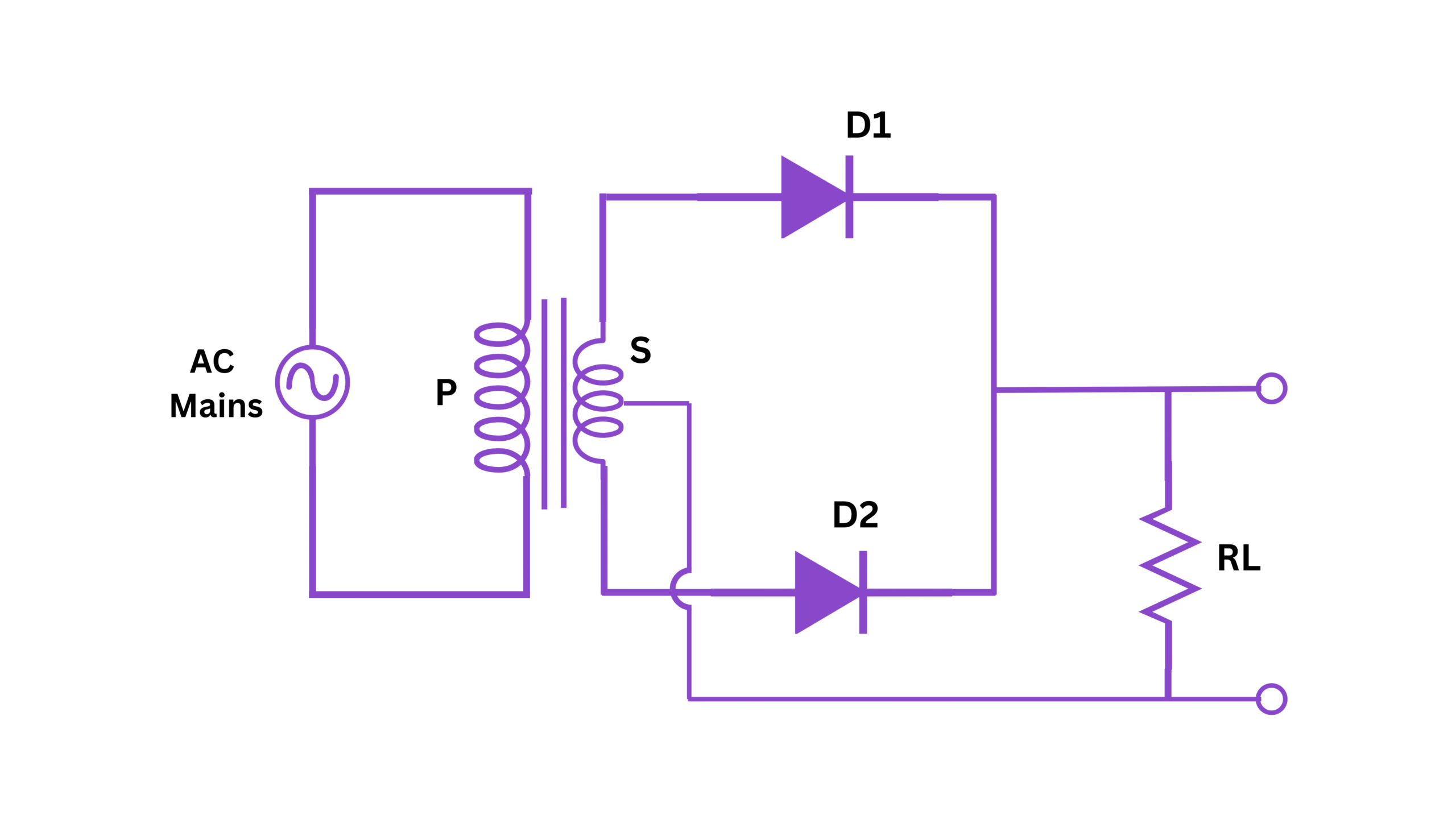
Fig. 1: Full Wave Rectifier Circuit using Center-Tapped Transformer
4. Theory
A full wave rectifier is a circuit that converts alternating current (AC) to direct current (DC) by utilizing both halves of the AC input waveform. Unlike a half-wave rectifier that only uses one half-cycle, a full wave rectifier rectifies both the positive and negative half-cycles of the input AC signal.
There are two common types of full wave rectifiers:
- Center-tapped transformer type: Uses a center-tapped transformer and two diodes
- Bridge type: Uses four diodes arranged in a bridge configuration
In this experiment, we focus on the center-tapped transformer type of full wave rectifier.
Working Principle:
The center-tapped full wave rectifier uses a transformer with a center-tapped secondary winding. This creates two equal but opposite voltages with respect to the center tap. Two diodes are connected such that each conducts during alternate half-cycles of the input.
During Positive Half-Cycle:
When the upper end of the secondary winding is positive with respect to the center tap, diode D₁ is forward-biased and conducts, while diode D₂ is reverse-biased and does not conduct. Current flows through D₁ and the load resistor RL.
During Negative Half-Cycle:
When the lower end of the secondary winding is positive with respect to the center tap, diode D₂ is forward-biased and conducts, while diode D₁ is reverse-biased and does not conduct. Current flows through D₂ and the load resistor RL.
In both cases, the current through the load resistor flows in the same direction, producing a pulsating DC output that utilizes both half-cycles of the input.
The main advantage of a full wave rectifier over a half-wave rectifier is its higher efficiency and lower ripple content in the output waveform.
5. Formula
Average Output Voltage (VDC):
Where Vm is the peak value of half secondary voltage.
RMS Output Voltage (VRMS):
Ripple Factor (r):
Form Factor:
Efficiency (η):
Peak Inverse Voltage (PIV):
6. Procedure
- Connect the circuit as shown in the diagram, ensuring that the center tap of the transformer is connected to ground.
- Set up the CRO to observe both input and output waveforms.
- Turn on the power supply and adjust to the required input voltage.
- Measure the RMS value of the input voltage across half of the secondary winding using a multimeter.
- Calculate the peak value of the half secondary voltage (Vm = √2 × VRMS-input).
- Observe and sketch the input and output waveforms on the CRO.
- Measure the DC output voltage across the load resistor using a multimeter set to DC mode.
- Measure the RMS output voltage across the load resistor using a multimeter set to AC mode.
- Vary the input voltage in steps and record the corresponding DC and RMS output voltages.
- Calculate the ripple factor, form factor, and efficiency for each set of readings.
- Turn off the power supply and disconnect the circuit.
7. Observation Table
| S.No. | Input Voltage (VRMS-input) (V) |
Peak Input Voltage (Vm) (V) |
DC Output Voltage (VDC) (V) |
RMS Output Voltage (VRMS) (V) |
Theoretical DC Voltage (V) |
Ripple Factor | Efficiency (%) |
|---|---|---|---|---|---|---|---|
| 1 | |||||||
| 2 | |||||||
| 3 | |||||||
| 4 | |||||||
| 5 |
8. Calculations
Sample Calculations:
-
Peak Input Voltage (Vm):
\[ V_m = \sqrt{2} \times V_{RMS-input} \] -
Theoretical DC Output Voltage:
\[ V_{DC-theoretical} = \frac{2V_m}{\pi} = 0.637V_m \] -
Ripple Factor (r):
\[ r = \sqrt{\left(\frac{V_{RMS}}{V_{DC}}\right)^2 - 1} \] -
Efficiency (η):
\[ \eta = \frac{(V_{DC})^2}{(V_{RMS})^2} \times 100\% \] -
Percentage Error in DC Output Voltage:
\[ \text{Error (\%)} = \frac{|V_{DC-theoretical} - V_{DC-measured}|}{V_{DC-theoretical}} \times 100\% \]
9. Result
- The full wave rectifier circuit without filter was successfully constructed and tested.
- Input and output waveforms were observed on the CRO and sketched.
- The average DC output voltage measured was _____ volts for an input RMS voltage of _____ volts.
- The experimental ripple factor was calculated to be _____.
- The experimental efficiency of the rectifier was found to be _____%, which is close to the theoretical value of 81.2%.
- The form factor of the full wave rectified output was _____, compared to the theoretical value of 1.11.
10. Precautions
- Ensure all connections are tight and correct before powering on the circuit.
- Use appropriate rating diodes that can handle the peak inverse voltage.
- Avoid touching the circuit when it is powered on.
- Ensure the load resistor has sufficient power rating to dissipate the heat generated.
- Check the polarity of diodes before connecting them in the circuit.
- Use a center-tapped transformer with proper voltage ratings.
- Do not exceed the rated voltage of the transformer.
- Ensure proper grounding of the oscilloscope to avoid electric shock.
- Make sure the measuring instruments are properly calibrated.
- Switch off the power supply when changing connections.
11. Viva Voice Questions
1. What is the difference between a half wave and full wave rectifier?
A half wave rectifier uses only one half (positive or negative) of the AC input waveform, while a full wave rectifier utilizes both halves of the AC input waveform. Full wave rectifiers are more efficient and produce less ripple in the output.
2. Why is the efficiency of a full wave rectifier higher than that of a half wave rectifier?
The efficiency of a full wave rectifier is higher (around 81.2%) compared to a half wave rectifier (around 40.6%) because it utilizes both half-cycles of the input AC waveform, resulting in better power transfer from the input to the output.
3. What is ripple factor and why is it important?
Ripple factor is a measure of the AC component present in the rectified output. It is defined as the ratio of the RMS value of the AC component to the DC value of the output. A lower ripple factor indicates a better DC output with less pulsation.
4. What is the Peak Inverse Voltage (PIV) in a full wave rectifier and why is it important?
Peak Inverse Voltage (PIV) is the maximum voltage that a diode must withstand when it is reverse biased. In a center-tapped full wave rectifier, PIV = 2Vm. It's important because diodes must be selected with a PIV rating higher than this value to prevent breakdown.
5. Why is a filter circuit often used with a rectifier?
A filter circuit is used to reduce the ripple content in the rectified output, providing a smoother DC voltage. Common filters include capacitor filters, inductor filters, and combination LC filters. Without a filter, the output contains significant pulsations.
6. What are the advantages of a bridge rectifier over a center-tapped full wave rectifier?
A bridge rectifier doesn't require a center-tapped transformer, has better transformer utilization, and subjects the diodes to a lower PIV (Vm compared to 2Vm in center-tapped). However, it uses four diodes instead of two.
7. How does diode forward voltage drop affect the output of a full wave rectifier?
The diode forward voltage drop (typically 0.7V for silicon diodes) reduces the output voltage of the rectifier. In a full wave rectifier, there is always one diode conducting, so the output is reduced by one diode drop at any time.
8. What would happen if the diodes in a full wave rectifier were connected with reversed polarity?
If the diodes were connected with reversed polarity, they would conduct during the wrong half-cycles, resulting in no output or potentially damaging the circuit components due to incorrect current flow.
9. Why is the form factor of a full wave rectified waveform different from that of a sine wave?
The form factor of a waveform is the ratio of RMS value to the average value. For a sine wave, it's 1.11, and for a full wave rectified sine wave, it's also 1.11. This is because the full wave rectification preserves the shape of each half-cycle of the sine wave, just making both half-cycles positive.
10. How does load resistance affect the performance of a full wave rectifier?
A higher load resistance draws less current, resulting in less voltage drop across the diodes and internal resistance of the transformer, leading to a higher output voltage. However, the power delivered to the load decreases. A lower load resistance increases the current but may cause more voltage drop in the circuit components.